A Collection of the Research
Previous works 2013-2015
Previous works 2007-2010
Research Topics (in Japanese)
最近の研究紹介
ニュースレター/News Letter No.1-3 (2007-2009)
ニュースレター/News Letter No. 4 (2015)
Photonics Innovation
A Collection of the Research 2013-

Interaction analysis between SFNPs and proteins. Each SFNPs was mixed with protein. The fluorescent spectrum of
supernatant monitored by excitation wavelength at 400 nm. (a) αGlc-SFNP, (b) αGlcNAc-SFNP, (c) βGal-SFNP, (d) ZAIS/ZnS stabilized with TGA.
Confocal laser scanning microscopic imaging of HepG2 cells. Overlay images (top panel, A−G) and fluorescence images (lower panel H−N). HepG2 cells were incubated without SFNPs (A and H) and with αGlc-SFNPs (B and I), αGlcNAc-SFNPs (C and J), βGal-SFNPs (D and K), SAα2−3Gal-SFNPs (F and M), or SAα2−6Gal-SFNPs (G and N).
|
Sugar chains play a significant role in various biological processes through sugar chain–protein and sugar chain–sugar chain interactions. To date, various tools for analyzing sugar chains biofunctions have been developed. Fluorescent nanoparticles (FNPs) functionalized with carbohydrate, such as quantum dots (QDs), are an attractive imaging tool for analyzing carbohydrate biofunctions in vitro and in vivo. Most FNPs, however, consist of highly toxic elements such as cadmium, tellurium, selenium, and so on, causing problems in long-term bioimaging because of their cytotoxicity. In this study, we developed cadmium-free sugar-chain-immobilized fluorescent nanoparticles (SFNPs) using ZnS-AgInS2 (ZAIS) solid solution nanoparticles (NPs) of low or negligible toxicity as core components, and investigated their bioavailability and cytotoxicity. SFNPs were prepared by mixing our originally developed sugar-chain-ligand conjugates with ZAIS/ZnS core/shell NPs. In binding experiments with lectin, the obtained ZAIS/ZnS SFNPs interacted with an appropriate lectin to give specific aggregates, and their binding interaction was visually and/or spectroscopically detected. In addition, these SFNPs were
successfully utilized for cytometry analysis and cellular imaging in which the cell was found to possess different sugar-binding properties. The results of the cytotoxicity assay indicated that SFNPs containing ZAIS/ZnS have much lower toxicity than those containing cadmium. These data strongly suggest that our designed SFNPs can be widely utilized in various biosensing applications involved in carbohydrates.
Cadmium-Free Sugar-Chain-Immobilized Fluorescent Nanoparticles Containing Low-Toxicity ZnS-AgInS2 Cores for Probing Lectin and Cells
Hiroyuki Shinchi, Masahiro Wakao, Nonoka Nagata, Masaya Sakamoto, Eiko Mochizuki, Taro Uematsu, Susumu Kuwabata, and Yasuo Suda
Bioconjugate Chem. 2014, 25, 286−295
|
|
|
We have developed a technique based on two-photon polymerization
lithography to fabricate arbitrary 3D structures in which aligned SWCNTs are embedded. SWCNTs are aligned along nanowires or laser scanning directions while they are embedded in the structure, as evidenced by polarized Raman microspectroscopy. The alignment is induced by spatial confi nement, volume shrinkage, and optical gradient force. The obtained composites, which exhibit the nematic order parameters up to 0.4, should lead to an enhancement of mechanical, electrical, thermal, and optical properties, as anisotropic properties resemble those of individual SWCNTs, thereby opening up possibilities of making devices and systems consisting of macroscopic ensembles of aligned SWCNT. Our method can also attain vertical alignment of SWCNTs if the laser is scanned along vertical direction. Further, the alignment along vertical direction would be also enhanced with tailoring polarization of the laser beam parallel to z -direction that is created by focusing radially polarized laser beam. Our method, thus, enables alignment control in any desired directions in arbitrary 3D nanostructures, which should lead to new applications such as actuators and metamaterials.
Direct Laser Writing of 3D Architectures of Aligned Carbon
Nanotubes
Shota Ushiba, Satoru Shoji, Kyoko Masui, Junichiro Kono, and
Satoshi Kawata
Adv. Mater. 2014, 26, 5653–5657
|
Schematic of the electro-optic effect in the miscible polymer/LC nanocomposite.
|
Demonstration of an optical amplitude modulator. Transient transmission curves of a He-Ne laser obtained from samples
after polymerization between crossed polarizers being driven by a 10 kHz sine wave.
|
We report a microsecond electro-optic response in an anisotropic-polymer/liquid-crystal composite, which forms a homogeneously mixed structure in the nanoscale range owing to the high miscibility between them. The nanocomposite was fabricated by photopolymerizing a nematic liquid crystal (NLC) mixture doped with a cross-linkable mesogenic monomer at a concentration of 30 wt%. Our system is inherently different from polymer-dispersed liquid crystals in that the LC molecules are almost miscible in the anisotropic polymer matrix and do not form observable domains. When an electric field is applied to such a nanocomposite, the molecular alignment of the polymer matrix is retained, while the non-polymerizable NLC reorients along the electric field, leading to a shift in the birefringence. Furthermore, the reorientation of the NLC molecules in a space sufficiently smaller than the wavelength of visible light results in scattering-free characteristics over the entire visible wavelength range and a short decay response time of 15 μs.
Nematic liquid crystal nanocomposite with scattering-free, microsecond electro-optic response
Yo Inoue, Hiroyuki Yoshida, and Masanori Ozaki
Optical Materials Express, Vol. 4, Issue 5, pp. 916-923 (2014)
|
|
|
Some highlights of our research results and activities are introduced. They include Plasmonic Imaging, Nano Plasmonic Devices, Biosensor Devices, Solar Cells, Functional Nanomaterials, Plasmaphotonics and CsLiB6O10 Crystal. Also introduced are activities for photonics industrialization and a platform for innovation: "Photonics Cannery" as well as international/domestic conferences/workshops, Photonics Days and weekly tea gathering. Contributions of Osaka University OSA/SPIE Student Chapter are also essential such as Asia Student Photonics Conferences and the Kid’s Photonics School “Super HIKARI JUKU”, an outreach program of the Photonics Center.
The Photonics Center
at Osaka University
Satoshi Kawata and Hiroshi Iwasaki
AAPPS BULLETIN february 2014 vol. 24 no. 1 P. 32
|
|

(a) A TERS image of two carbon nanotubes crossing each other in “X” shape (X-CNT sample), where the x-y plane indicates the sample plane, the color represents TERS intensity of the G + mode in accordance with the color bar shown on the left, and the z axis shows the value of the Fano parameter |1/q|, which corresponds to the degree of semiconductor-to-metal transition. (b) A line profile of |1/q| along the yellow dashed line in (a). (c) White dashed lines depict the location of the nanotubes in the X-CNT sample, whereas the colored spots indicate the TERS intensity of a new Raman mode centered at 1607 cm -1, which arise due to the local reduction of radial symmetry, in accordance with the color bar on the left.
|
The electronic properties of single walled carbon nanotubes (SWNTs) can change with a slight deformation, such as the one caused by the pressure of one SWNT crossing over the other in an ‘‘X’’ shape. The effect, however, is extremely localized. We present a tip-enhanced Raman investigation of the extremely localized semiconductor-to-metal transition of SWNTs in such a situation, where we can see how the Fano interaction, which is a Raman signature of metallic behavior, grows towards the junction and is localized within a few nanometers of its vicinity. After exploring the deconvoluted components of the G-band Raman mode, we were able to reveal the change in electronic properties of a SWNT at extremely high spatial resolution along its length.
Tip-Enhanced Raman Investigation of Extremely Localized Semiconductor-to-Metal Transition of a Carbon Nanotube
Yoshito Okuno, Yuika Saito, Satoshi Kawata, and Prabhat Verma
PRL 111, 216101 (2013)
|
|
Point-spread-function (PSF) of scattering from isolated gold nanoparticles evolves with increasing excitation intensity. The left column shows backscattering images and the right column gives the signal profile of a selected nanoparticle (white dashed line). The red circles are experimental values and green lines are Gaussian fitting. (a) When the excitation intensity is low, the PSF fits well to a Gaussian profile. (b) As the intensity is higher than 105 W/cm 2, the top of PSF becomes flattened, manifesting the onset of saturation. (c) With intensity keeps increasing, the saturation effect is stronger, resulting in the very interesting PSF that the center is lower than peripheral. The widths of the side lobes are about 40 nm. (d) When the intensity is higher than 106 W/cm 2, the scattering signal at the center of PSF increases again, revealing the onset of reverse saturation. (e) The reverse saturated scattering quickly dominates the PSF as the excitation continues to increase. The FWHM of the reverse saturated part is about 100 nm, showing great potential for high-resolution microscopy. Scale bar: 500 nm.
|
Nonlinear optical interaction is crucial to all optical signal processing. In metallic nanostructures, both linear and nonlinear optical interactions can be greatly enhanced by surface plasmon resonance (SPR). In the last few decades, saturation and reverse saturation of absorption in plasmonic materials have been unraveled. It is known that scattering is one of the fundamental light−matter interactions and is particularly strong in metallic nanoparticles due to SPR. However, previous methods measure response from ensemble of nanoparticles and did not characterize scattering on a single particle basis. Here we report that backscattering from an isolated gold nanoparticle exhibits not only saturation, but also reverse saturation. Wavelength-dependent and intensity dependent studies reveal that nonlinear scattering is dominated by SPR and shares a similar physical origin with nonlinear absorption. The reversibility and repeatability of saturable scattering (SS) and reverse saturable scattering (RSS) are validated via repetitive excitation on the same set of particles. Compared to fluorescence, our novel discovery of single-particle-based SS and RSS does not suffer from bleaching and can be used as a more robust contrast agent for optical microscopy. Under a reflection confocal microscope, interesting point-spread functions are observed, with full-width-of-half-maximum of central and side lobes reduced to λ/5 and λ/13, showing great potential for super resolution microscopy.
Saturation and reverse saturation of scattering in a single plasmonic nanoparticle
Shi-Wei Chu, Hsueh-Yu Wu, Yen-Ta Huang, Tung-Yu Su, Hsuan Lee, Yasuo Yonemaru, Masahito Yamanaka, Ryosuke Oketani, Satoshi Kawata, Satoru Shoji, and Katsumasa Fujita
ACS Photonics, Article ASAP (2013)
|
|
Fluorescence images of HeLa cells cultured in a three-dimensional (3-D) matrix and the line profiles of the structures. (a) SAX and (c) confocal images of actin filaments in HeLa cells in the x–z plane. (b and d) Magnifications of the boxed area in (a and c). The line profiles are shown in (e and f) of the structures indicated by the arrows in the adjacent images. The sample was stained with ATTO488 phalloidin, and the pixel size was 175 nm. The pixel numbers were 400 × 270 for (a and c) and 50 × 100 for (b and d), the pixel dwell time was 500 μs, and the excitation intensities for SAX and confocal modes were 12 and 1.2 kW∕cm 2, respectively. A silicone-oil immersion 1.3 NA objective lens was used with a pinhole size corresponding to 0.5 Airy units. In addition, low-pass filtering was applied to the images.
|
Saturated excitation (SAX) microscopy offers high-depth discrimination predominantly due to nonlinearity in the fluorescence response induced by the SAX. Calculation of the optical transfer functions and the edge responses for SAX microscopy revealed the contrast improvement of high-spatial frequency components in the sample structure and the effective reduction of background signals from the out-of-focus planes. Experimental observations of the edge response and x-z cross-sectional images of stained HeLa cells agreed well with theoretical investigations. We applied SAX microscopy to the imaging of three-dimensional cultured cell clusters and confirmed the resolution improvement at a depth of 40 μm. This study shows the potential of SAX microscopy for super-resolution imaging of deep parts of biological specimens.
Saturated excitation microscopy for sub-diffraction-limited imaging of cell clusters
Masahito Yamanaka, Yasuo Yonemaru, Shogo Kawano, Kumiko Uegaki, Nicholas I. Smith, Satoshi Kawata, and Katsumasa Fujita
J. Biomed. Opt., Vol. 18, 126002 (2013)
|
|
Raman imaging of protonated and deprotonated forms of FCCP in live HeLa cells. Raman images were obtained from HeLa cells treated with 100 uM FCCP. The signals at 2197 and 2230 cm -1 were assigned to the red and green channels, respectively, and a merged image was generated. The laser wavelength was 532 nm. The light intensity at the sample plane was 4.2 mW/um 2. The exposure time for each line was 10 sec. The total number of lines was 140.
|
We report the simultaneous imaging of protonated and deprotonated forms of carbonylcyanide p-trifluoromethoxyphenylhydrazone (FCCP) molecules in live cells by Raman microscopy. Nitrile, a structure-sensitive Raman tag, is used to detect the two distinct molecular structures, demonstrating the potential of Raman microscopy for structure-based imaging of bioactive small molecules.
Simultaneous imaging of protonated and deprotonated carbonylcyanide p-trifluoromethoxyphenylhydrazone in live cells by Raman microscopy
Hiroyuki Yamakoshi, Almar F. Palonpon, Kosuke Dodo, Jun Ando, Satoshi Kawata, Katsumasa Fujita, and Mikiko Sodeoka
Chem. Commun., Accepted Manuscript (2013)
|
|
(a) Measured thermal radiation spectra of the SRRs and the substrate. (b) Simulated electric field distributions in the SRR structure at the peak positions in (a). Ex and Ey are linear polarizations that are parallel and perpendicular to the SRR gap, respectively. kz is the direction of the radiation, which is normal to the substrate. au: Arbitrary units. m: Mode number.
|
An array of split-ring resonators efficiently absorbs and re-emits thermal energy as IR radiation to power thermophotovoltaic (TPV) systems. We have designed, constructed, and tested a metamaterial made of an array of SRRs that is an effective heat–light converter with a controllable spectrum and low heat capacity.
A metamaterial to convert heat to light
Yosuke Ueba and Junichi Takahara
SPIE Newsroom 10.1117/2.1201310.005129
|
|
Simulated results of electric field intensity (|E| 2 on the Ag surface) in a tapered lossless silver slab waveguide with h = 30nm: (a) selective excitation of ss 0 mode in both sides with phase difference of 0 and (b) selective excitation of sa 0 mode in both sides with phase difference of π. Note that each scale bar is normalized by the field maximum. The maxima are not equal each other.
|
A symmetric metal slab waveguide simultaneously supports two opposite types of propagation mode similar to a metal film: short-range surface plasmon (SRSP) like mode and long-range surface plasmon (LRSP) like mode. The strong field confinement of SRSP-like mode plays a crucial role for nano-optical integrated circuits in spite of short propagation length. In order to avoid the trade-off between field confinement and propagation length, we demonstrate selective mode excitation and mutual mode conversion for nanofocusing mediated by LRSP-like mode.
Mutual mode control of short- and long-range surface plasmons
Junichi Takahara and Masashi Miyata
Focused Issue(Surface Plasmon Photonics)/Optics Express, Vol. 21, Issue 22, pp. 27402-27410
|
|
(a) Two-dimensional colour image of a nanotube manipulated into the shape of the word ‘CNT’. This image was constructed by colour coding the frequency position of G+-mode in TERS spectra. The colour variation shows strain distribution along the nanotube at high spatial resolution. For comparison, TERS images of the same sample were constructed from (b) the intensity of G+-mode and (c) simultaneously obtained AFM topography.
|
Tip-enhanced Raman scattering microscopy is a powerful technique for analysing nanomaterials at high spatial resolution far beyond the diffraction limit of light. However, imaging of intrinsic properties of materials such as individual molecules or local structures has not yet been achieved even with a tip-enhanced Raman scattering microscope. Here we demonstrate colourcoded tip-enhanced Raman scattering imaging of strain distribution along the length of a carbon nanotube. The strain is induced by dragging the nanotube with an atomic force microscope tip. A silver-coated nanotip is employed to enhance and
detect Raman scattering from specific locations of the nanotube directly under the tip apex, representing deformation of its molecular alignment because of the existence of local strain. Our technique remarkably provides an insight into localized variations of structural properties in nanomaterials, which could prove useful for a variety of applications of carbon nanotubes and other nanomaterials as functional devices and materials.
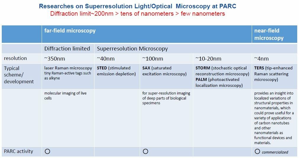
Tip-enhanced nano-Raman analytical imaging of locally induced strain distribution in carbon nanotubes
Taka-aki Yano, Taro Ichimura, Shota Kuwahara, Fekhra H’Dhili, Kazumasa Uetsuki, Yoshito Okuno, Prabhat Verma &
Satoshi Kawata
Nature Communications 4, Article number: 2592
|
|
Raman images of alkyne-tagged cell 3D micro/nano structural SWCNT/polymer
composites are fabricated by using the TPP lithography. The structures in (a)–(f) are a 8-lm-long micro bull, a micro tea
pod, a micro lizard, a nanowire suspended between two micro boxes, magnified image of (d), and perspective view of the nanowire, respectively.
|
We have demonstrated a method for 3D micro/nano-fabrication of SWCNT/polymer composites by the two-photon polymerization (TPP) lithography. We showed that SWCNTs were fully and uniformly embedded into micro/nano-structures. In addition, we found that SWCNTs were aligned along the nanowire axis. Furthermore, the spatial resolution for fabrication was as small as 200 nm in lateral direction, which is much higher than that reported for other fabrication processes for the 3D structural composites. The resultant structures would exhibit higher mechanical and electrical properties, especially in a nowire shaped composites, due to the self-alignment of SWCNTs inside the wire. These results indicate that our method is promising for realizing SWCNT/polymer composite-based 3D MEMS and NEMS.
3D microfabrication of single-wall carbon nanotube/polymer composites by two-photon polymerization lithography
Shota Ushiba, Satoru Shoji, Kyoko Masui, Preeya Kuray, Junichiro
Kono, Satoshi Kawata
CARBON 59 (2013) 283
|
|
Raman images of alkyne-tagged cell proliferation probe, EdU, in HeLa cells. (a–d) These show the distribution of signal
corresponding to 749 (a), 1685 (b), 2123 (c) and 2856 cm − 1 (d). (e) The overlay image was constructed by merging the images at 749, 2123 and 2856 cm − 1, which are assigned to the green, blue and red channels, respectively. The excitation laser wavelength was 532 nm. The light intensity at the sample was 3.3 mW μm − 2. The exposure time for each line was 10 s. The total number of lines of exposure was 192, and the images consist of 192 × 280 pixels. (f) Average Raman spectra from the cytoplasm, nucleus and extracellular region. a.u., arbitrary units.
|
A protocol is given for constructing and using a Raman microscope equipped with both a slit-scanning excitation and detection system (high temporal and spatial resolution) and a laser steering and nanoparticle-tracking system (dynamic surface-enhanced Raman imaging using gold nanoparticles). Both features enable mapping of the distributions of molecules in live cells and visualization of cellular transport pathways. Furthermore, its utility can be expanded to small-molecule imaging by using tiny Raman-active tags such as alkyne. For example, DNANA synthesis in a cell can be visualized by detecting 5-ethynyl-2′
-deoxyuridine (EdU), a deoxyuridine derivative with an alkyne moiety. We describe the optics, hardware and software to construct the Raman microscope, and discuss the conditions and parameters involved in live-cell imaging. The whole system can be built in ~8 h.
Raman and SERS microscopy for molecular imaging of live cells
Almar F Palonpon, Jun Ando, Hiroyuki Yamakoshi, Kosuke Dodo, Mikiko Sodeoka, Satoshi Kawata & Katsumasa Fujita
nature protocols 690 | VOL.8 NO.4 | 2013 |
|
|
Osteoclasts are bone resorbing, multinucleate cells that differentiate from mononuclear macrophage/monocyte-lineage hematopoietic precursor cells (:Large multinucleated cell responsible for the dissolution and absorption of bone 破骨細胞). Although previous studies have revealed important molecular signals, how the bone resorptive functions of such cells are controlled in vivo remains less well characterized. Here, we visualized fluorescently labeled mature osteoclasts in intact mouse bone tissues using intravital multiphoton microscopy. Within this mature population, we observed cells with distinct motility behaviors and function, with the relative proportion of static – bone resorptive (R) to moving – nonresorptive (N) varying in accordance with the pathophysiological conditions of the bone. We also found that rapid application of the osteoclast-activation factor RANKL converted many N osteoclasts to R, suggesting a novel point of action in RANKL-mediated control of mature osteoclast function. Furthermore, we showed that Th17 cells, a subset of RANKL-expressing CD4+ T cells, could induce rapid N-to-R conversion of mature osteoclasts via cell-cell contact. These findings provide new insights into the activities of mature osteoclasts in situ and identify actions of RANKL-expressing Th17 cells in inflammatory bone destruction.

The interaction between Th17 and osteoclast depends on RANKL expressed on Th17.
(A) Intravital multiphoton imaging (low-power view) of osteoclasts (green) in mouse bone tissues of a3-GFP mice after administration of in vitro–differentiated Th1 (labeled with CMF2HC — blue) and Th17 (labeled with CMTPX — red) (Supplemental Video 7). Cell borders are marked by white lines. Scale bar: 40 μm. (B) The migratory behaviors of Th1 and Th17. Blue and red spheres represent Th1 and Th17 cells, respectively, and white lines show the associated trajectories. Scale bar: 40 μm. (C) Summary of mean tracking velocities of Th1 and Th17 cells. Data points (n = 10 for Th1, and n = 48 for Th17) represent individual cells compiled from 3 independent experiments. (D) The number of Th1 or Th17 cells attached to mature osteoclasts for more than 5 minutes (n = 4, from 3 independent experiments). (E) Summary of mean tracking velocity of Th17 cells treated with isotype control antibody or anti-RANKL antibody. Data points (n = 32 for Th17 cells treated with isotype control antibody and n = 30 for Th17 cells treated with anti-RANKL antibody) represent individual cells compiled from 3 independent experiments. (F) The number of Th17 cells treated with isotype control antibody or anti-RANKL antibody attached to mature osteoclasts for more than 5 minutes (n = 5, from 3 independent experiments).
Dynamic Visualization of RANKL and Th17-mediated Control of Osteoclast Function
Junichi Kikuta, Yoh Wada, Toshiyuki Kowada, Ge-Hong Sun-Wada, Issei Nishiyama, Shin Mizukami, Nobuhiko Maiya, Hisataka, Yasuda, Atsushi Kumanogoh, Kazuya Kikuchi, Ronald Germain, Masaru Ishii
J. Clin. Invest., 123, 866-873 (2013)
|
|
|
Schematic of the QD-based plasmon emitter. SPPs can be excited directly by illuminated QDs, resulting in the emission from an output slit.
(a) SIM image of the structure. The structural parameters are the same as for Fig. 2(e). (b) Fluorescence image with an excitation laser focused onto the QD layer. The arrow shows the polarization of an excitation laser.
|
We have experimentally demonstrated the design of functional and controllably integrated QD-based plasmon emitters coupled to a thin metal film supporting long-range (∼ 35 μm), lowdispersion and two-dimensional isotropic plasmon guiding. The QD-based plasmon emitters analysed here have high potential for power-efficient emitters, and can also be applied to a wide range of frequencies by selection of QD size and composition.
Our concept will be implemented with a plasmon emitter coupled to other planar plasmonic waveguides with same configurations such as metal slab plasmonic waveguides and dielectric-loaded plasmonic waveguides; these waveguides are now one of the best options for plasmonic routing and processing. Furthermore, the emitter can be integrated with other QD-based components, such as modulators and amplifiers with similar dimensions, in one-chip circuits by using our fabrication technique. We believe that the present work will be the basis of these applications and offer further development of a wide range of plasmonics.
Colloidal quantum dot-based plasmon emitters with planar
integration and long-range guiding
Masashi Miyata and Junichi Takahara
8 April 2013 / Vol. 21, No. 7 / OPTICS EXPRESS 7882
|
|
|
|
IDEC and Nitto Denko, both are PARC member companies, successfully invented a new fast and reliable LED production process. A series of LED sealing process (5 steps) that took 6 hours could be replaced by a two steps process of 40 min by utilizing an newly developed gel resin sheet. The new method enabled more uniform device sealing compared to the conventional one.
Extreme Prehardened Sheet Sealed (EX-PRESS) Method
NIKKEI MONOZUKURI March 2013 pp.22 (in Japanese)
|
|
|
|
Plasma resonance in metals exhibits some unique optical phenomena that occur on the surface of metal with nanostructures. The use of surface plasmons has been proposed in various fields, such as nanometer-resolution near-field optical microscopy, nanoscale optical circuits, single molecule detection, molecular sensors, cancer treatment, solar cells, lasers, and holography. The study of plasma resonance is called “plasmonics” and is expected as a new field of nanophotonics. In this report, I review the principles and limits of plasmonics and give a future outlook. Challenging breakthroughs are discussed.
COMPREHENSIVE REVIEW
Plasmonics: Future Outlook
Satoshi Kawata
Japanese Journal of Applied Physics 52 (2013) 010001
|
|