

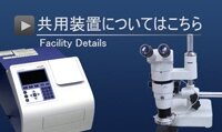


◆パートナー企業の方向けの共用装置について◆
フォトニクスの産業創出・イノベーションに供するための最先端の加工・分析・評価・設計ツールを350㎡の実験室(この内クリーンルーム100㎡)に整備しています。
本センターのメンバー・パートナー企業が利用できます。これらの装置を利用するには申請が必要です。また利用時毎に予約が必要です。予約はこちらから
装置に関するご質問・お問い合わせは、までお気軽にご連絡ください。
The 350 m2 laboratory is equipped with the most advanced processing, analysis, evaluation and design tools devoted to photonics industry creation and innovation, including a 100 m2 clean room. This center is for the use of member and partner companies. An application is required to use this equipment. A reservation is also necessary each time.
|
P3-205
3次元のモデルを、樹脂を堆積させ作成する装置です。試作品のモックアップ(実物とほぼ同様に似せて作られた模型)などに用います。3Dモデルを輪切りにしたデータにしたがい、自動でインクジェット樹脂吹きつけ・紫外線硬化により造形します。大きさは、340x340x200mm以下。
This device fabricates three-dimensional models in sophisticated detail with structures of less than 20 μm. It is used for mockups and prototypes. The model is formed by automatically spraying plastic through inkjet and hardening it with ultraviolet, based on numeric data. The size of the models is less than 340 x 340 x 200 mm.
NC加工装置 Numerically

ファナック/ROBODRILL α-D21MiA5
光学機器などの高精度を要する金属や樹脂製部品を、数値制御(NC)により切削加工する装置です。プログラムを組むことで自動で高速・微細な加工が行えます。
This device machines components such as optical mounts requiring high precision, using numerical control (NC). The operational data (NC program) for drilling is entered. The accuracy of positioning of the drill axis is 0.006 mm, and the maximum size that can be machined is 500 x 400 x 330 mm (vertical).

構造設計ソフト Structural Design Software
Solid Works / Solid Works Professional
部品、組み立て品の3Dモデルや設計図を作成できる3次元CADソフトウェアです。複雑な自由曲面を用意に描画でき、JISやISOに準拠したボルト・ナット・ピンなどのライブラリも利用できます。製品の動きをリアルに表現するアニメーションの作成も可能です。
This three-dimensional CAD software can create design drawings for actual product-level components and assemblies. It covers modeling functions for complex free form surfaces, precision sheet metal processing, plastics and so on, and it has standard libraries for JIS and ISO-compliant bolts, nuts, pins, parts libraries for bearings, retaining rings and the like, and functions for preparing cam shapes. It can also create realistic animations of the movement of products.

光学系設計ソフト Optical Design Software
Zemax/Zemax 13 IE
光学設計・評価ソフトウェア。レンズ設計、LEDなどの照明設計、ディスプレイ、集光型太陽電池、レーザー光伝搬、迷光、光ファイバーなど、あらゆる光学系のモデル化、解析、最適化、および公差解析などの光学設計に利用できます。
This software is for optical design and evaluation. It can be used for the design of lenses, LEDs and other lighting, as well as modeling, analysis, optimization and tolerance analysis of all sorts of optical systems, including displays, concentrating solar cells, laser light propagation, stray light, optical fiber and the like.
アイデックス/BF-100UT
輸送時などの製品損傷(動作不良・割れ・こすれ・静電気・傷など)を再現する装置で送試験の結果は梱包材及び商品の損傷対策に利用できます。3軸同時振動、試験テーブル800×1000mm、120kg搭載可能。
This equipment reproduces damage to products during shipping, including operational defects, cracking, friction, static electricity, and scratches. The results of shipping tests can be used for developing packing materials and protective measures. The 800 × 1,000 mm testing table can oscillate in three axes simultaneously and support up to 120 kg.
P3-517 薄膜デバイス作成室(クリーンルーム) Thin Film Device Fabrication Lab (Clean room)

マスクレス露光装置 Maskless Lithography
ナノソリューションズ/DL-1000
CADで作画したパターンデータを、フォトマスクを用いることなく直接基板上のフォトレジストに露光できます。また、グレースケール露光によりレジストの三次元加工も可能です。露光光源は波長405nmのLEDで試料サイズは数mm四方~5インチウェハーまで対応。最小画素1μm。
Pattern data created with CAD can be used to expose photoresist directly on the substrate without using a photomask. Furthermore, three dimensional processing of the resist is possible using grayscale exposure. The exposure light source is LED with a wavelength of 405 nm, and sample sizes from several millimeters square to 5-inch wafers are supported. The smallest pixel is 1 μm. |
P2-212

Focused Ion Beam System FB2200
日立ハイテク/FB2200
イオンビームによりサンプルの微細加工・観察を行います。高速かつ大面積加工が可能で、2048×2048ピクセル以下のBMPを読み込んでの加工や試料を薄く基削りだし拾い上げるマイクロサンプリング・カーボンやタングステンを堆積させるデポジション機能を備えます。像分解能は6nm以下、倍率は60~300,000倍、最大加工観察範囲:30×30mm。
This equipment is for micromachining and observing samples with an ion beam. It enables high-speed large area manufacturing, and can perform processing and micro sampling by reading a bitmap of 2,048 × 2,048 pixels or less.Image resolution is 6 nm or less, magnification is 60 to 300,000 times, and maximum processing and observation range is 30 × 30 mm.

コンパクトスパッタ Compact Suputter
アルバック/ACS-4000
コンパクトスパッタは物質に薄膜を付ける装置です。スパッタリングという製膜方法により化合物薄膜や多層膜を生成します。
本装置はパソコンによる自動プロセスと、4インチの基盤に対応しています。金属(Au,Cr,Tiなど)やカーボンを成膜することができます。
Equipment for forming thin films of metal and other substances on a 2-inch substrate. The film material target is bombarded with argon ions produced by electric discharge, and the material particles accumulate on the substrate. Besides metals, carbon, quartz and other materials can be applied as films, and three types of target can be used at the same time.

紫外可視近赤外分光光度計 UV-VIS-NIR Spectrophotometer
島津製作所/UV-3600
185~3300nmの波長域から紫外・可視・近赤外領域に分けた光を試料に照射し、透過もしくは反射した光の強度を検出して試料の吸光度・透過率および反射率を測定する装置。波長の最高分解0.1nm。
Equipment that irradiates a sample with light divided into ultraviolet, visible, and near-infrared regions from a wavelength region of 185 to 3,300 nm. It detects the intensity of the transmitted or reflected light to measure the absorbance, transmittance and reflection coefficient of the sample. The maximum resolution of the wavelength is 0.1 nm.
P2-211 光学評価室
Optical Characterization Lab
 非接触表面形状・粗さ測定器 Laser Interferometer 非接触表面形状・粗さ測定器 Laser Interferometer
ZYGO/ VeriFire-XPZ
光学部品などの平面または球面の面精度の測定を、干渉作用を利用して、高速、高精度に行います。光学平面基板、レンズ、プリズムなどのガラスやプラスチック光学部品、コンピュータディスクやベアリングのような精密金属部品等が測定できます。幅10cmの測定物を高低差30nmの精度で測定できます。
This equipment uses interference to measure the profile irregularity of the planar or spherical surfaces of optical components and so on, at high speed with high precision. It can measure optical planar substrates, lenses, prisms and other glass and plastic optical components, as well as precision metal components such as computer disks and bearings and the like. It is capable of measuring height differences with accuracy of 0.5 nm in objects with a width of 10 cm.

接触型表面形状・粗さ測定器 Surface Profiler
KLA-Tencor/ P-16+
基板やレンズなどの表面をダイアモンドの針でなぞり、表面の粗さ、段差、微小なうねり、全体の形状を測定し、2次元及び3次元解析を行う装置です。最大サンプルサイズ 200mm、最大操作距離80mm、段差測定再現性 1nm以下。
This equipment traces the surface of a substrate or lens with a diamond needle, measuring the whole shape including surface roughness, differences in height, and minute swellings, performing two and three-dimensional analysis. The maximum sample size is 200 mm, and height difference measurement reproducibility is down to 1 nm or smaller.

デスクトップ型ナノリソグラフィ装置・AFM Nanolithography Device・AFM
nanoINK/DPN5000
様々な種類のプローブを使用することにより、基板上のナノ構造に液体を流し込んだり塗布することができます。プローブはペン先が1本のものから10x10本のアレイ状のものまであり、一度の工程で大量の塗布も可能です。針を利用しナノ精度でのAFM(原子間力顕微鏡)観察も可能です。
Using various kinds of probe, AFM (atomic force microscope) measurement at nanoscale accuracy and washing nanostructures on substrates with fluid and coating them is possible. Probes can be a single pen tip, or an array of 10 x 10, applying a large amount in a single process.
ハイロックス/ KH-8700
試料を35~5000倍で観察・計測できるマイクロスコープです。観察部の3Dモデル構築や画像連結による広範囲撮影、表面粗さやポイント高さの計測、ラインプロファイルの表示等の機能により試料の観察・評価を手軽に行えます。
Capable of observing and measuring specimens at 35x to 5000x magnification. 3D model creation and image linking in the observation unit enable photography in a wide range. Features such as surface roughness and point height measurement and line profile display make it easy to observe and evaluate specimens.
|
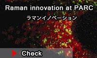
P3-309

レーザーラマン顕微鏡 Laser Raman Microscope Nanophoton/RAMAN-11
物質や細胞のラマン散乱光を測定し画像を得ることの出来る装置です。ラマン散乱光とは光が分子に当たって散乱される光です。試料における特定の物質の組成分析や結晶構造、分子情報を得ることが可能です。
This device measures the Raman light scattering of substances and cells, giving an image. Raman light scattering is the scattering of light when light hits a molecule. It is possible to perform composition analysis of specific substances in the sample, identify the crystal structure and obtain molecular information.

共焦点レーザースキャニング顕微鏡 Confocal Laser Scannning Microscope ニコン/A1R MR
細胞や組織を鮮明な画像として観察することの出来る顕微鏡です。試料の蛍光を検出し画像を作成します。また、スライス状に取得した画像を三次元構築し、立体画像として作成することも可能です。4基のレーザーを同時照射可能。
This microscope enables observation of cells and tissues as a clear image. It detects the fluorescence of the sample and creates an image. In addition, it is possible to build three-dimensional images from images captured as slices. Laser wavelength is 405/457•477•488•514/561/638 nm and the laser scanning range is about 2.7 × 12.7 mm.

Waters /1525/432/2475/2998
溶液中に溶け込んだ化合物を分離・分析する装置です。複雑な化合物の混合溶液から特定の物質を分離精製することも可能です。特にこの装置は高速で分離・精製を行うことが出来ます。
This is a device for separating and analyzing compounds dissolved in liquid. It is also possible to separate and purify specific substances from mixed solutions of complex compounds. This equipment can separate and purify substances at high speed.

LC-MS Waters/UPLC Xevo Q-Tofシステム
有機合成における中間合成化合物、最終生成物質の確認、薬物のスクリーニングからDNA、タンパク質などの生体高分子まで対応した質量分析装置です。高速液体クロマトグラフ(LC)と組み合わせることで、多数の成分からなる分析対象物に対しても、高速・高感度で質量分析を行うことができます。
This is a mass spectrometer that can check intermediate synthetic compounds and final product substances in organic synthesis, as well as screening for drugs and analyzing biopolymers such as DNA and proteins. By combining it with a high-speed liquid chromatograph (LC), it can perform mass spectrometry of analytical subjects formed of many components, at high speed with high sensitivity.

DNAシーケンサーDNA Sequencer 3500
Applied Biosystems 3500
蛍光ベースの全自動DNA解析システムで、DNAの塩基配列解析、フラグメント解析や個人診断解析についてサンプルのロードから一次データ解析までの手順を完全自動で行うことができます。
This a fluorescence-based fully automatic DNA analysis system. For DNA sequencing analysis, fragment analysis, or individual diagnostic analysis, it performs every step from loading the samples to primary data analysis completely automatically.
サーマルサイクラー
Veriti サーマルサイクラー Applied Biosystem

ポリメラーゼ連鎖反応(PCR)によりDNA断片を複製させるための機械です。正確な温度制御で再現性良くDNA断片を複製することができ、独立した6つのブロックゾーンで異なる温度を設定・運転することができます。
サーモサイエンティフィック/Multiskan GO
200-1000nmの幅広い波長域から任意の波長を選択しアッセイや処理量に合

わせた吸光度測定をキュベット・マイクロプレートの両方で行うことができます。
Able to select the desired wavelength in a wide wavelength region (200 - 1000 nm) and perform absorbance measurements that are designed for a particular assay and processing volume, using either cuvettes or microplates.
分析天秤 超純水製造システム
Water Purification Sysytem

ドラフトチャンバー 製氷機
Fume Hood Flake Ice Maker

|


